Saturday, April 26, 2008

AMD's Asset Smart Explained

Although Hector Ruiz mentioned the term Asset Smart at the Q1 2008 Earnings Report he avoided explaining what it meant. There has been a lot of speculation in this vacuum but all of it that I have seen has been wrong. Most theories seem to focus on either the idea of selling all or part of a FAB to raise cash or on the idea of making graphic products at Dresden. It is actually something quite different.

Asset Smart deals with manufacturing. Starting from 1998 you have:

1998 - SPC
2000 - APC
2003 - APM
2005 - LEAN
2008 - SMART

The term Asset Light referred to AMD's changes within the Lean project (although some of these had actually started back with the APM project). The next project is SMART. Asset Smart simply refers to similar changes within the Smart project which begins in Q3 2008. Mostly, these projects deal with the process of making chips and trying to reduce manufacturing costs. The groundwork for this next phase was actually begun by AMD back in June of 2007 during SEMICON West when it hosted meetings of the Next Generation Factory (NGF) group. This continued during ISMI in October 2007 and later at SEMICON Japan. For example Semiconductor International covers the Austin meeting here:

In an effort to place a more intense focus on 300 mm fab productivity improvements, Advanced Micro Devices Inc. (AMD, Sunnyvale, Calif.) is hosting ~75 people at its Austin campus today for the second in a series of Next Generation Factory (NGF) meetings.

The day-long Austin meeting will include particpants from six integrated device manufacturers — AMD, Freescale Semiconductor, IBM, Qimonda, Renesas Technologies and Spansion — and 16 semiconductor equipment vendors, said Gerald Goff, senior member of AMD’s technical staff. Six academic experts in fab productivity were also expected to attend, Goff said prior to the meeting.

“The suppliers and IDMs used to work more directly together on productivity issues,” Goff said, adding that the NGF group is intended to complement efforts within SEMI and the International Sematech Manufacturing Initiative (ISMI). “ISMI is not moving fast enough. We have to push this 300 mm fab efficiency issue harder as an industry,” Goff said, adding that ISMI project manager Denis Fandel will be among the attendees at today’s event. “In no way do we want the takeaway from this to be that we are against ISMI,” he said, adding, however, that the growing industry emphasis on 450 mm wafers is “concerning to us.”

Goff said that because AMD was “relatively late getting to 300 mm wafers,” it may have more interest in productivity gains at the 300 mm wafer size than its competitor, Intel Corp. (Santa Clara, Calif.), which seeks momentum behind the transition to 450 mm wafers in ~2012.


You can get more information about this directly from AMD by looking at Doug Grose's Keynote Presentation at the 4th ISMI Symposium.

Back in 1998 AMD was at 2.5 days per mask layer. After SPC, APC, and APM, FAB 30 was down to 1.5 days per mask layer. With Lean, by the time FAB 30 shut down in mid 2007 it was down to just 1 day per mask layer. What AMD wants to do is reduce cost by reducing cycle time just as it has been doing for the past 10 years. As a result of Lean, wafer starts per week have jumped 31%, while labor productivity (monthly activities per operator) has climbed 72%. Monthly wafer costs have dropped 26%, and the already mentioned cycle time per mask layer has been trimmed 23%. However, FAB 36 is still at 1.4 days per mask layer. AMD is hoping to reduce this down to 0.7 days per mask layer (a 50% reduction) by shifting to small lot manufacturing.

The basic strategy involves replacing batch tooling with single wafer tooling and reducing batch size. AMD wants to drop below the current batch size of 25 wafers. AMD figures that this will dramatically reduce Queue Time between process steps as well as reduce the actual raw process time. Overall AMD figures a 76% reduction in cycle time is possible so a 50% reduction should be reasonable. Today, running off a batch of 25 wafers is perhaps 6,000 dies. Reducing batch size would allow AMD to catch problems sooner and allow much easier manufacturing of smaller volume chips like server chips. Faster cycle time means more chips with the same tooling. It also means a smaller inventory because orders can be filled faster and smaller batches mean that AMD can make its supply chain leaner. All of these things reduce cost and this is exactly how AMD plans to get its financial house in order.

Monday, April 14, 2008

Updates And Old Patterns

Amid AMD's torrent of bad news: the exit of Phil Hester, the reduced estimates for Q1 Earnings, and the announced 10% layoffs we can at least give AMD a small amount of praise for getting the B3 stepping out the door. It's a small step on a long road.

We can finally settle the question of whether AMD's 65nm process is broken. AMD's fastest 65 watt, 90nm K8 runs 2.6Ghz while the fastest 65 watt, 65nm K8 runs 2.7Ghz. So, the 65nm process is at least a little better than the old 90nm process. People still keep clamoring for Ruiz to step down. Frankly, I doubt Ruiz had any direct involvement with K10's design or development so I'm not sure what this would accomplish. I think a better strategy would be for AMD to get the 2.6Ghz 9950 out the door as soon as possible and try hard to deliver at least a 2.6Ghz Shanghai in Q3. Since Shanghai has slightly higher IPC a 2.6Ghz model should be as fast or faster than a 2.7Ghz Barcelona. I would say that AMD needs at least that this year although this would leave Intel with the top three slots.

AMD's current strategy seems to recognize that they are not competitive at the top and won't get there soon. The collection of quads without L3 cache, Tri-core processors, and the current crop of low priced quads including the 9850 Black Edition all point to a low end strategy. This is the same pattern AMD fell into back in 2002 when it devalued its K7 processors. Of course in 2002 AMD didn't have competitive mobile and its only server processors were Athlon MP. So perhaps Puma and a genuine volume of B3 Opterons will help. AMD's excellent 7xx series chipset should help as well but apparently not enough to get back into profitability without layoffs.

The faster B3 steppings are an improvement but you get the feeling they should have been here last year. You get a similar feeling when Intel talks about the next Itanium release. Although Itanium began with hope as a new generation architecture its perpetual delays keep that feeling well suppressed. And, one has to wonder how much of Itanium will be left standing when Intel implements AVX in 2010. We all know that HP is the only thing holding up Itanium at this point. Any reduction in support by HP will be the end of Itanium. And, we get a similar feeling about Intel's 4-way offerings which always seem to lag nearly a year behind everything else. For example, although Nehalem will be released in late 2008 the 4-way version of Nehalem won't come out until late 2009. Some still speculate that this difference is purely artificial and Intel's way of giving Itanium some breathing room.

However, as bad as AVX might be for Itanium it has to be a double shock for AMD coming not long after the announcement of SSE5. AVX seeks to copy SSE5's 3 and 4 operand instructions while bumping the data width all the way up to 256 bits. It looks like AMD only has two choices at this point. They can either drop SSE5 and adopt both SSE4 and AVX or they can continue with SSE5 and try to extend with GPU instructions. Following AVX would be safer but would put AMD behind since it is unlikely at this point that they could optimize Bulldozer for AVX. Sticking with SSE5 and adding GPU extensions would be a braver move but could work out better if AMD has its Fusion ducks in a row. Either way, Intel's decision is likely to fuel speculation that Larrabee's architecture isn't strong enough for its own Fusion type design. Really though it is tough to say at this point since stream type processing is just beginning to take off. However, GPU processing does demonstrate sheer brute power on Folding @ Home protein sampling. This makes one wonder why OC'ers in particular cling to the use of SuperPi which is based on quaint but outdated x87 instructions as a comparative benchmark.

There is also the question of where memory is headed. Intel is already running into this limitation with Nehalem where only the server and top end chips will get three memory channels. I'm sure Intel had intended that the mid desktop would get three as well, but without FBDIMM three channels would make the motherboards too expensive. This really doesn't leave Intel anywhere to go to get more bandwidth. Supposedly, AMD will begin shifting to G3MX which should easily it to match three or even four channels. However, it isn't clear at this point if AMD intends G3MX on the desktop or just the servers and high end like Intel. With extra speed from DDR3 this shift probably doesn't have to happen in 2009 but something like this seems inevitable by 2010.

Saturday, March 08, 2008

45nm, An Interesting Convergence In Design

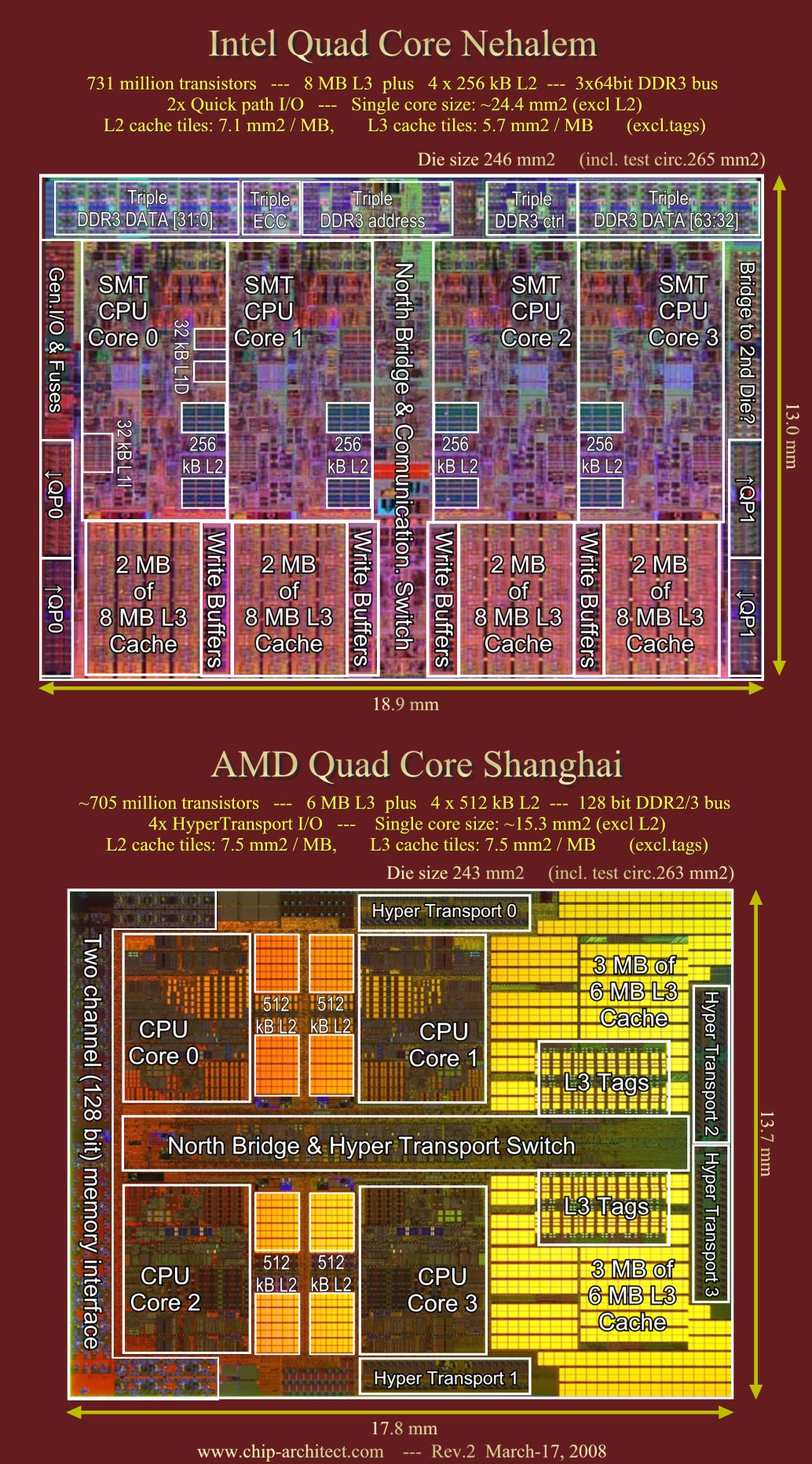
AMD's K8 has been trailing C2D for the past 18 months. Making things worse, AMD has stumbled a bit with its K10 launch while Intel's Penryn seems to be on schedule. It is somewhat surprising then to discover that Intel's Nahelem and AMD's Shanghai are so similar.


Both are quad core, both use L3 cache, and both use a point to point interface (QuickPath for Intel and HyperTransport for AMD). And, according to Hans De Vries:

Nehalem
731 Million Transistors
246mm Die Size
7.1mm/MB L2 Cache Density

Shanghai
700 Million Transistors
243mm Die Size
7.5mm/MB L2 Cache Density

We don't really see much difference until we look at core size and L3 density:

Nehalem
24.4mm Core Size
5.7mm/MB L3 Cache Density

Shanghai
15.3mm Core Size
7.5mm/MB L3 Cache Density

AMD uses 2MB's of L2 + 6MB's of L3 for 8MB's total.
Intel uses 1MB of L2 + 8MB's of L3 for 9MB's total.

Along with similar total cache size the area devoted to cache is similar as well (nearly identical area for L3). However, the area devoted to core logic is quite different:

Nehalem
Core Area - 97.6mm
L2 Area - 7.1mm
L3 Area - 45.6mm

Shanghai
Core Area - 61.2mm
L2 Area - 15mm
L3 Area - 45mm

We see right away that Nehalem devotes 85% more die area to core logic than to cache whereas Shanghai devotes about the same die area to core logic and cache. It is almost a certainty that with Nehalem's greater amount of core transistors that it will run faster than Shanghai. On the other hand it should also consume more power. If we assume that Intel gets a reduction in power draw due to having better 45nm transistors then this should offset some of Nehalem's higher power draw. However, with 60% more transistors devoted to core logic I don't believe that all of this could be offset. My guess is that at full load Nehalem will draw more than Shanghai but Nehalem should be closer at idle power. Actually, Nehalem's core ratio at 40% is almost the same as Penryn's at 41% which is only slightly less than Merom's at 44%. In contrast, Shanghai's core ratio has dropped to a tiny 25% much smaller than Barcelona's 36%.

Penryn has a density of 6.0mm/MB for L2. Therefore, I would expect Nehalem's L2 at a density of 7.1mm/MB to be faster than Penryn's L2. However, I would also expect Nehalem's L3 at 5.7mm/MB to be slightly slower than Penryn's L2. This is interesting because we know that Barcelona's L3 is a bit slow. However, with an L2 twice the size of Nehalem's this should be a closer match than Barcelona is to current Penryn with its massive 12MB L2. Essentially, Shanghai is Barcelona with 3X the L3 cache but Nehalem's cache structure is much more like Shanghai's than Penryn's. Shanghai is unlikely to have any significant core changes from Barcelona but there may be some minor changes in the decoding section. This is pretty much what I would expect. Since Barcelona only improved on the decoding speed of FP instructions compared to K8 I would expect AMD to tweak a few more Integer instructions in Shanghai to increase speed. Decreasing decoding time for commonly used instructions would also make a lot of sense given Penryn's advantage in decoders. AMD is not likely to get a boost of 10-15% doing this but a boost of, say, 3% is possible. AMD might see another 3% boost in speed due to larger L3 although this could possibly be higher if AMD could make L3 faster. A lot of people are wondering if AMD will bump the master L3 clock on Shanghai for better performance at speeds above 2.3Ghz. Just bumping the clock could be worth another 1%. So, I'm guessing a total speedup for Shanghai of perhaps 7% versus Barcelona.

There is one other obvious difference in the die layout. Shanghai has mirror image cores. This means that a master clock signal originating from the center of the Northbridge area should propagate out to each of the four cores at the same time and this is a standard way of doing timing. However, since Nehalem's cores are placed side by side it must be using a more sophisticated clocking scheme. In other words, there is not any place on the Nehalem die where a clock signal would reach all four cores at the same time. This would tend to suggest the possibility that each core actually has its own master clock allowing them to run nearly asynchronously. If Nehalem does indeed have this ability then this could be a big benefit in offsetting the higher power draw since cores that were less busy could simply be clock scaled downward. AMD could therefore be in for a tough fight in 2009 in spite of the similarities between Shanghai and Nehalem. The one big benefit to AMD from the similarity is that it makes it nearly impossible to cache tune the benchmarks in Intel's favor. This means that Intel is probably going to lose some artificial advantage that it has now with Penryn. However, given the difference in core transistors and Nehalem's greater memory bandwidth I can't see any reason why Nehalem couldn't make up for this loss and still have an overall performance lead at the same clock as Shanghai.